
IC-280E - Empfänger ICOM - Kostenlose Bedienungsanleitung
Finden Sie kostenlos die Bedienungsanleitung des Geräts IC-280E ICOM als PDF.


Benutzerfragen zu IC-280E ICOM
0 Frage zu diesem Gerät. Beantworten Sie die, die Sie kennen, oder stellen Sie Ihre eigene.
Eine neue Frage zu diesem Gerät stellen
Laden Sie die Anleitung für Ihr Empfänger kostenlos im PDF-Format! Finden Sie Ihr Handbuch IC-280E - ICOM und nehmen Sie Ihr elektronisches Gerät wieder in die Hand. Auf dieser Seite sind alle Dokumente veröffentlicht, die für die Verwendung Ihres Geräts notwendig sind. IC-280E von der Marke ICOM.
BEDIENUNGSANLEITUNG IC-280E ICOM
IC-280E
144MHz FM TRANSCEIVER
INSTRUCTION MANUAL
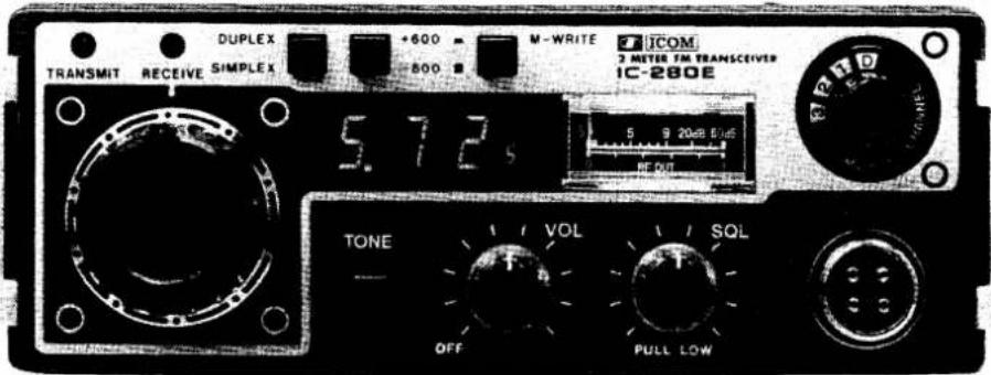
text_image
TRANSMIT RECEIVE DUPLEX +600 M-WRITE ICOM SIMPLEX 800 2 METER FM TRANSCEIVER IC-280E 5.72s TONE VOL SQL OFF PULL LOWTABLE OF CONTENTS
I. SPECIFICATIONS .... 1
II. DESCRIPTION.... 2
III. INSTALLATION 3
IV. CONTROL FUNCTIONS.... 6
V. OPERATION 8
VI. INSIDE VIEW 10
VII. THEORY OF OPERATION 12
VIII. TROUBLE SHOOTING.... 17
IX. VOLTAGE CHARTS.... 18
X. BLOCK DIAGRAM 21
XI. OPTION 22
XII. P.C. BOARD LAYOUT.... 23
SECTION I SPECIFICATIONS
GENERAL
| Numbers of semi-conductors | : Transistors 38FET 4IC 27Diode 49 |
| Frequency coverage | : 144.000 ~ 146.000MHz : 25KHz steps |
| Memory channels | : 3 channels, any inband frequency programmable |
| Usable conditions | : Temperature: -10°C - 60°C (14°F - 140°F)Operationable time: continuous |
| Frequency stability | : Within ±1.5KHz |
| Antenna impedance | : 50 ohms unbalanced |
| Power supply requirement | : 13.8V DC ±15% (negative ground) 3.0A Max. |
| Current drain | : TransmittingHIGH. (10W) Approx. 2.5ALow (1W) Approx. 1.2AReceivingAt max audio output Approx. 0.7ASquelched Approx. 0.5A |
| Dimensions | : 156mm (W) x 58mm (H) x 228mm (D) |
| Weight | : Approx. 2.2kg |
TRANSMITTER
| Output power | : 10W (HIGH), 1W (LOW) |
| Emission mode | : 16F_3 |
| Modulation system | : Variable reactance frequency modulation |
| Max. frequency deviation | : ±5KHz |
| Spurious emission | : More than 60dB below carrier |
| Microphone | : 600 ohms dynamic microphone with push-to-talk switch (IC-SM2 electret condenser microphone may also be used.) |
| Operating mode | : Simplex, Duplex (±600KHz from receive frequency) |
RECEIVER
| Receiving system | : Double-conversion superheterodyne |
| Modulation acceptance | : 16F3 |
| Intermediate frequency* | : 1st: 10.695MHz2nd: 455KHz |
| Sensitivity | : More than 30dB S+N+D/N+D at 1μVLess than 0.6μV for 20dB Noise quieting |
| Squelch sensitivity | : Less than 0.4μV |
| Spurious response rejection ratio | : More than 60dB |
| Selectivity | : More than ±7.5KHz at -6dB pointLess than ±15KHz at -60dB point |
| Audio output power | : More than 2.0W |
| Audio output impedance | : 8 ohms |
Use of Microcomputer
This IC-280E is the world's first amateur transceiver with a P-channel MOS 4-bit microcomputer. Frequency control, band-edge detection, and the display are accomplished by the microcomputer. The 3-channel memory is controlled electrically by the use of a 256-bit RAM area. The circuits for these IC-280E functions are equivalent in capability to conventional circuits having a large number of C-MOS MSI's.
Separable Control Unit
The control portion (front panel) of the IC-280E can be separated from the rest of the unit, and the two parts can be connected with a cable. The control unit is approximately one-third of the whole unit; therefore, the IC-280E can be easily mounted almost anywhere in a car.
Superior Receiving Characteristics
The use of newly developed low-noise and large dynamic range junction FET's (for the RF amplifier and the first mixer) and of helical cavity filters (for the antenna and RF circuits) provides excellent sensitivity and intermodulation distortion characteristics. A pair of high quality monolithic crystal filters facilitates very stable receiving and excellent durability.
Highly Stable Transmitting Characteristics
Both the directly amplified VCO output without the use of multipliers or mixers and the use of a power module in the PA unit produce very clean transmitting signals without spurious radiation. RF power is selectable 10W (HIGH) and 1W (LOW).
Unpacking:
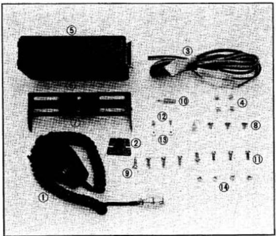
Carefully remove your transceiver from the packing carton and examine it for signs of shipping damage. Should any be apparent, notify the delivering carrier or dealer immediately, stating the full extent of the damage. It is recommended you keep the shipping cartons. In the event storage, moving, or reshipment becomes necessary, they come in handy. Accessory hardware, cables, etc., are packed with the transceiver. Make sure you have not overlooked anything.
text_image
Labeled diagram of a medical or electronic device with numbered components including a device, cable, and connectors.- Microphone (dynamic type) 1
- Microphone hook 1
- Power cord 1
- Spare fuses (5A) 2
- Installing holder A 1
- Installing holder B 1
-
Installing angle joint 1
-
Gimp screws 4
- Flat washers 12
- Plug for speaker 1
- Mounting screws 8
- Screws for additional bracket 2
- Flat head screw's nuts 2
- Mounting screw's nuts 4
Location:
Where you place the transceiver in your automobile is not critical and should be governed by convenience and accessibility. Since the unit is so compact, many mobile possibilities present themselves. In general, the mobile mounting bracket will provide you with some guide as to placement. Any place where it can be mounted with metal screws, bolts, or pop-rivets will work. For fixed station use, a power supply should be designed to produce 3 amps for the transceiver.
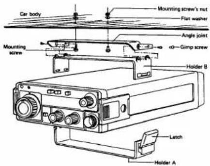
Mounting bracket installation
text_image
Car body Mounting screw's nut Flat washer Mounting screw Angle joint Gimp screw Holder B Latch Holder ATransceiver installation
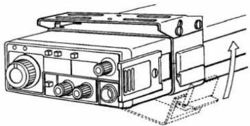
natural_image
Technical line drawing of a mechanical device with ports and a directional arrow indicating motion (no text or symbols)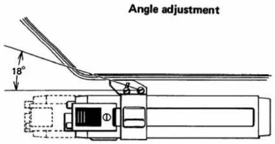
text_image
Angle adjustment 18°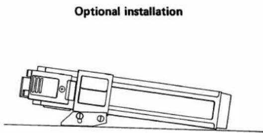
text_image
Optional installationPower Requirements:
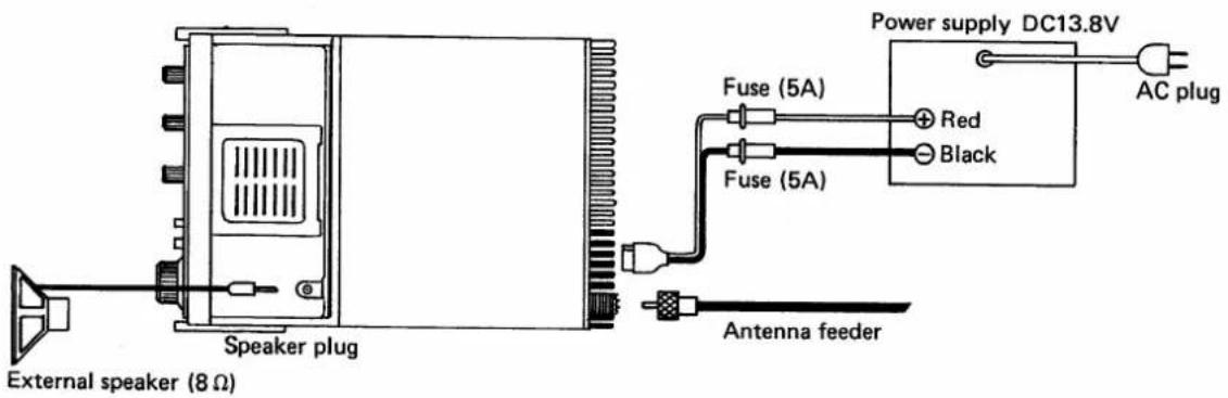
The transceiver is supplied ready to operate from any regulated 13.8V DC, 3 ampere negative ground source. An automobile 12 volt, negative ground, system is usually more than adequate. Some note must be taken, however, of the condition of the vehicle's electrical system. Items such as low battery, worn generator/alternator, poor voltage regulator, etc., will impair operation of your transceiver as well as the vehicle. High noise generation or low voltage delivery can be traced to these deficiencies. If an AC power supply other than the matching ICOM AC power supply is used with your transceiver, make certain it is adequately regulated for both voltage and current. Low voltage while under load will not produce satisfactory results from your transceiver. Receiver gain and transmitter output will be greatly impaired. Caution against catastrophic failure of the power supply should be observed.
CAUTION: Excessive Voltage (above 15VDC) will cause damage to your transceiver. Be sure to check source voltage before plugging in the power cord.
Included with your transceiver is a DC power cable with plug attached. The Red Wire is positive (+), the Black, negative (−). If your mobile installation permits, it is best to connect these directly to the battery terminals. This arrangement eliminates random noise and transient spikes sometimes found springing from automotive accessory wiring. If such an arrangement is not possible, then any convenient B+ lead in the interior of the vehicle and the negative frame can be utilized. Remember, the unit operates on a negative ground system only; it cannot be used in a positive ground automobile. After making your connections, simply insert the plug into your transceiver. When your transceiver is mated with its matching ICOM AC power supply, the power cable is simply plugged in the same receptacle in the transceiver and the AC line cord into any convenient wall receptacle.
text_image
External speaker (8 Ω) Speaker plug Power supply DC13.8V AC plug Fuse (5A) Red Black Fuse (5A) Antenna feederAntenna:
The most important single item that will influence the performance of any communication system is the antenna. For that reason, a good, high-quality, gain antenna of 50 ohms impedance is recommended, fixed or mobile. In VHF as well as the low bands, every watt of ERP makes some difference. Therefore, 10 watts average output plus 3dB of gain antenna equals 20 watts ERP, presuming low VSWR of course. The few more dollars invested in a gain type antenna is well worth it. When adjusting your antenna, whether mobile or fixed, by all means follow the manufacturer's instructions. There are some pitfalls to be aware of. For example, do not attempt to adjust an antenna for lowest VSWR when using a diode VSWR meter not engineered for VHF applications. Such readings will invariably have an error of 40% or more. Instead, use an in line watt meter similar to the Drake WV-4, Bird Model 43 or Sierra Model 164B with VHF cartridge. Further, when adjusting a mobile antenna, do so with the motor running preferably above normal idling speed. This will insure proper voltage level to the transceiver.
The RF coaxial connector on the rear chassis mates with a standard PL-259 connector. Some models may have metric threads. In any event, the RF connector will mate with almost any PL-259 connector if care is taken to seat them properly.
Microphone:
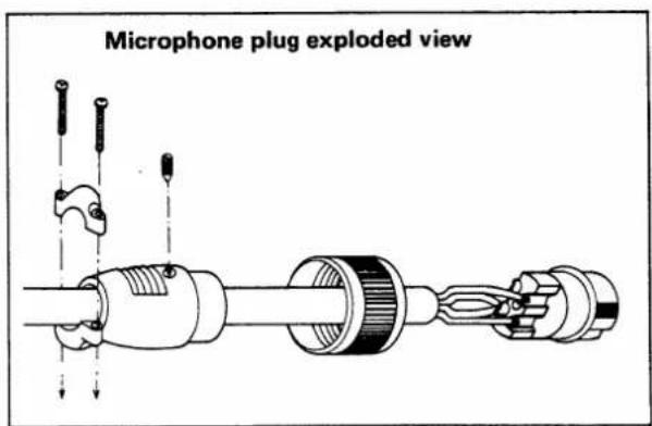
A high quality dynamic microphone is supplied with your transceiver. Merely plug it into the proper receptacle on the front panel. Should you wish to use a different microphone, make certain it is approximately 600 ohms. Particular care should be exercised in wiring also, as the internal electronic switching system is dependent upon it. See the schematic for the proper hook up.
text_image
Microphone plug exploded view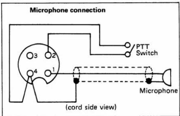
text_image
Microphone connection 3 2 4 1 (cord side view) PTT Switch MicrophoneExternal Speaker:
An external speaker jack and plug is supplied with your unit in the event another speaker is desirable. The external speaker impedance should be 8 ohms, and when used, will disable the internal speaker. An 8 ohm headset can be utilized as well.
SECTION IV CONTROL FUNCTIONS
FRONT VIEW
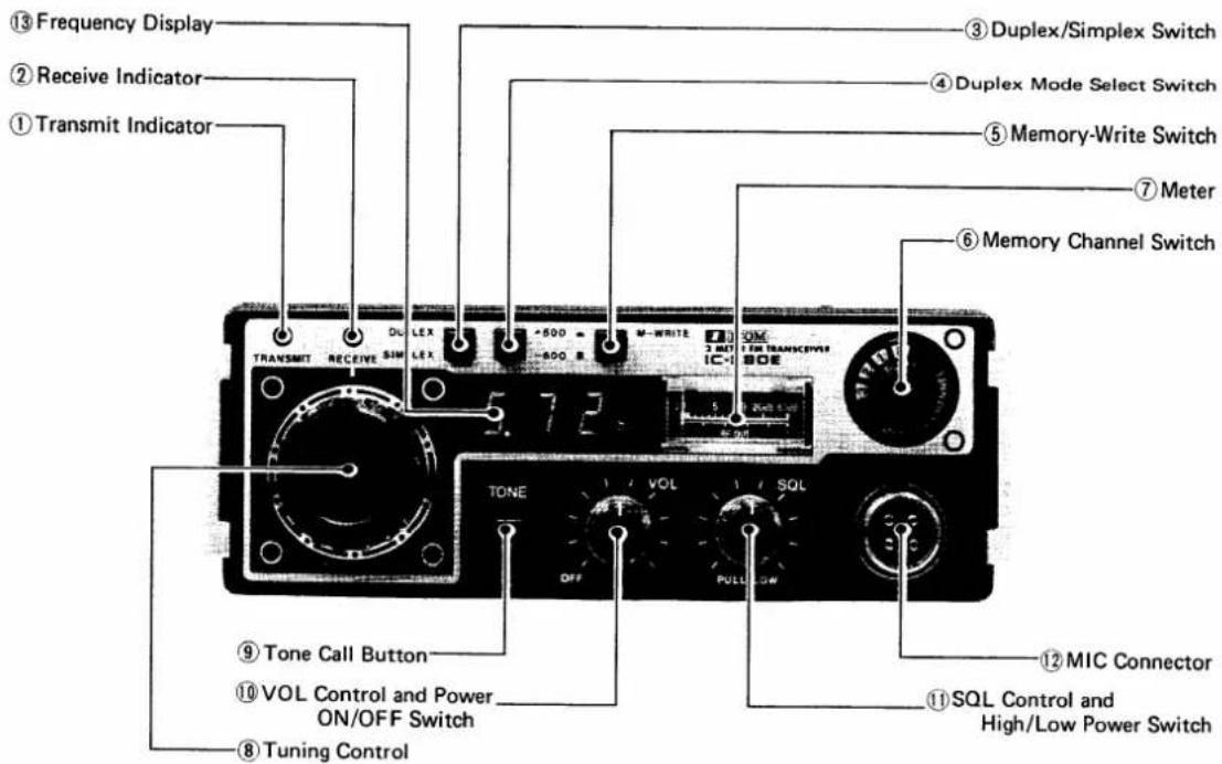
text_image
⑬ Frequency Display ② Receive Indicator ① Transmit Indicator ③ Duplex/Simplex Switch ④ Duplex Mode Select Switch ⑤ Memory-Write Switch ⑦ Meter ⑥ Memory Channel Switch TRANSMIT RECEIVE SIMLEX 5 7 2 M-WRITE 3 MET IC- ON FOR TRANSCEVER BOE TONE OFF VOL PULLLOW ⑨ Tone Call Button ⑩ VOL Control and Power ON/OFF Switch ⑧ Tuning Control ⑫ MIC Connector ⑪ SQL Control and High/Low Power Switch- Transmit Indicator: Illuminates in the transmit mode.
- Receive Indicator: Illuminates in the receive mode. (When squelch opened).
- Duplex/Simplex Switch: Selects Duplex or Simplex operation.
- Duplex Mode Select Switch: Sets the transmitting frequency 600KHz above or 600KHz below the receiving frequency in Duplex operation.
- Memory-Write Switch: To insert the desired frequencies into any of three Memory channels.
- Memory Channel Switch: To select operation with the tuning control or the memory channels.
- Meter: Functions both as a signal strength meter (S-meter) and as a relative RF output meter.
- Tuning Control: Sets the operating frequency.
- Tone Call Button: Actuates the tone call circuit for repeater operation.
- VOL Control and Power ON/OFF Switch: Controls audio level and turns the unit ON or OFF.
- SQL Control and High/Low Power Switch: Controls squelch threshold level, and sets the RF output power to 10 watts or 1 watt.
- MIC Connector: Accepts microphone plug.
- Frequency Display: Digitally displays the operating frequency.
BACK VIEW
- Antenna Connector: Accepts standard PL-259 coaxial connector.
- Power Connector: Mates with DC cord plug.
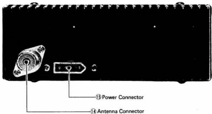
text_image
⑮ Power Connector ⑭ Antenna ConnectorCONTROL INSTRUCTIONS
Duplex/Simplex Select Switch
For repeater use, set this switch to the Duplex position by depressing to the locked in position. By depressing again, the switch returns to the out position for Simplex operation.
Duplex Mode Select Switch
There are two modes for repeater operation. With most repeaters, the required transmitting frequency (repeater input frequency) is 600KHz below the receiving frequency (repeater output frequency). This switch is to select 600KHz below or 600KHz above the receiving frequency. When the switch is locked in by depressing it, the transmitting frequency is set at 600KHz above the receiving frequency and reversed when the switch is in the out position by depressing again. In Simplex mode, this switch may be set at either position.
Memory-Write Switch
After setting the tuning control to the desired frequency with the Memory Channel switch in the "D" position, set the Memory Channel switch to the channel to be programmed (1, 2 or 3). One push of the M-Write switch erases the previous programmed frequency and programs the new frequency. (Depressing the M-Write switch when the Memory Channel switch is set at "D" neither erases nor programs a frequency.)
Memory Channel Switch
Selects operation with the tuning control ("D" position) or operation with the memory channels (1, 2 or 3). See "PROGRAMMING THE MEMORY CHANNELS" on page 9 for more details.
Meter
The numbers on the S-meter represent S1 through S9 and 20, 40 and 60dB over S9. The RF output level meter functions only as a relative output meter and does not indicate the wattage. These functions are switched automatically when T/R switching is made.
Tuning Control
The tuning control sets the operating frequency in 25KHz steps. This dial has 50 positions per turn.
Tone Call Button
Most repeaters require a 1750Hz Tone-burst for initial access. In the transmitting mode, by depressing the Tone Call Button for the required period for a repeater, the tone burst generator actuates and you can access the repeater.
VOL Control and Power ON/OFF Switch
When the control is turned completely CCW, the power is OFF. By turning the control CW beyond the "click", the unit is turned ON and the audio level increases by further rotating it CW.
SQL Control and High/Low Power Switch
Turning this control CW sets the squelch threshold higher. To turn OFF the SQL function, turn this control completely CCW. By pulling the Squelch control knob, the RF output power is reduced to 1 watt. By depressing the knob to the normal position, the RF output power returns to 10 watts.
Frequency Display
The three large digital LED's represent 1MHz, 100KHz and 10KHz digits. When the 5KHz display is needed, a small "5" is illuminated at the bottom right corner of the frequency display.
Initial Preparations:
Make sure the VOL Control and Power ON/OFF Switch is in the OFF position, then connect the power supply cord to the power connector. The red lead should be connected to the positive side of the power source and the black lead to the negative side. In the event that these leads are improperly connected, the transceiver will not function. Reversing polarity will blow out the fuse in the power supply cord due to actuation of the protective circuit.
Connect the microphone to the MIC Connector.
Connect the antenna to the Antenna Connector. Make sure the coax line is of the correct impedance (50 ohms) and is neither shorted nor open.
Turn the squelch control to the maximum counter-clockwise position.
RECEIVING
Set the controls and switches as follows:
⑥ MEMORY CHANNEL SWITCH
"D" position
⑪ SQL Control and High/Low Power Switch
completely CCW
(Others may be at any position or setting.)
Turn the VOL control clockwise (it will "click" ON) and the meter will illuminate with the frequency display showing "5.00" for 145.00MHz.
Turn the VOL control clockwise to a comfortable audio level.
If no signal can be heard but only noise, turn the SQL control clockwise until the noise from the speaker stops and set it just below this threshold. (When adjusting the SQL control setting, if some communication signals can be heard, turn the tuning control either direction and set it where only noise can be heard.)
Turn the tuning control to the desired frequency.
TRANSMITTING
Set the controls and switches as follows:
③ DUPLEX/SIMPLEX SWITCH
(see below)
④ DUPLEX MODE SWITCH
(see below)
⑧ Tuning control
desired frequency
⑪ SQL Control and High/Low Power Switch
HIGH (Normal position)
For simplex operation, set ③ DUPLEX/SIMPLEX SWITCH at the SIMPLEX position, making ④ DUPLEX MODE SWITCH nonfunctioning.
For repeater operation, set ③ DUPLEX/SIMPLEX SWITCH at DUPLEX and select whether the transmitting frequency is to be 600KHz above or below the receiving frequency. The -600KHz is normal for most repeaters.
If the lower output power is sufficient, set ⑪ SQL Control and High/Low Power Switch to the LOW (out) position.
Depress the PTT switch on the microphone for transmitting and release for receiving. Speak into the microphone with your normal speech level for the proper microphone level.
If you need a tone-burst for initial access of the repeater, depress the ⑨ Tone Call Button for the required period. (Tone-burst periods vary individually from 100mS to 2S.)
PROGRAMMING THE MEMORY CHANNELS
All of the following settings must be made while in the receive mode.
While the ⑥ Memory Channel Switch is set at the "D" position, turn ⑧ Tuning Control so that the frequency for programming is shown on ⑬ Frequency Display.
Set ⑥ Memory Channel Switch at the channel on which you would like to program (1, 2 or 3). If no frequency has been programmed, ⑬ Frequency Display shows "5.00". If another frequency has been programmed, the previously programmed frequency is shown on the Frequency Display.
Depress ⑤ Memory-Write Switch; The Frequency Display shows the frequency you set with ⑧ Tuning Control. At the same time, "5.00" or the previously programmed frequency is cancelled. This completes the programming.
The other two Memory Channels can be programmed in the same manner. Now you can operate using the Tuning Control plus the 3 programmed channels.
(TOP)
text_image
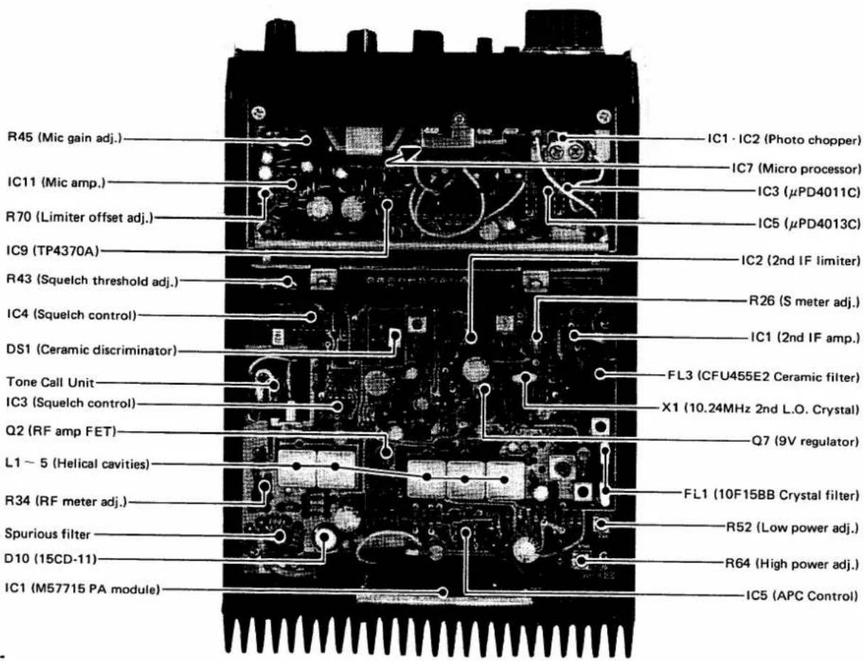
R45 (Mic gain adj.) IC11 (Mic amp.) R70 (Limiter offset adj.) IC9 (TP4370A) R43 (Squelch threshold adj.) IC4 (Squelch control) DS1 (Ceramic discriminator) Tone Call Unit IC3 (Squelch control) Q2 (RF amp FET) L1 ~ 5 (Helical cavities) R34 (RF meter adj.) Spurious filter D10 (15CD-11) IC1 (M57715 PA module) IC1 · IC2 (Photo chopper) IC7 (Micro processor) IC3 (μPD4011C) IC5 (μPD4013C) IC2 (2nd IF limiter) R26 (S meter adj.) IC1 (2nd IF amp.) FL3 (CFU455E2 Ceramic filter) X1 (10.24MHz 2nd L.O. Crystal) Q7 (9V regulator) FL1 (10F15BB Crystal filter) R52 (Low power adj.) R64 (High power adj.) IC5 (APC Control)General
The IC-280E has a digital Phase Locked Loop circuit for its local oscillator.
The PLL circuit is controlled with a programmed microcomputer developed by ICOM.
The band edges, memory channels and duplex setting are programmed in the computer.
The received signal is mixed with the output signal of the PLL circuit and converted into the 10.695MHz IF signal. This signal goes into a crystal filter to reject any nearby signals and then is mixed with the 10.24MHz signal, which is also used as the reference frequency signal for the PLL circuit, and converted to a 455KHz IF signal. After it is amplified, the signal is fed to the ceramic discriminator for demodulation.
In the transmit mode, the output frequency of the PLL circuit is shifted to the transmitting frequency and the signal is amplified up to 10 watts with the PA module. Frequency modulation is accomplished in the PLL oscillating circuit.
RECEIVING UNIT
Antenna Switching Circuit
The antenna connector is connected to the antenna switching circuit on the main board through the low-pass filter. In the receive mode, Q1 is turned ON and D1, D2 and D3 are conducted for RF signals by the current flow. The RF signal through this circuit is fed to the RF amplifier circuit.
RF Circuit
Signals filtered by the two-stage helical cavity filter which reduces interference and inter-modulation from other radio signals or nearby signals are amplified by Q2. The output signals through the three-stage helical cavity filter are fed to the gate of the first mixer Q3, which mixes the input signals with the local oscillator signals supplied at the source of Q3 from the PLL circuit to convert them to the first IF signals on 10.695MHz. To provide minimum cross modulation and desensitisation, a newly developed large dynamic range and low-noise junction FET is used for the first mixer as well as for the RF amplifier.
IF Circuit
IF signals from the drain of Q3 are filtered by a crystal filter and fed to the gate of the second mixer Q4. The reference frequency signal of the PLL circuit is used for the local oscillator signal of the second mixer. The signals are converted to 455KHz signals appear at the drain of Q4 and are amplified about 50dB by IC1 after being filtered by a high-quality ceramic filter. Then the signals are amplified about 5 - 15dB by the variable amplification amplifier Q5.
The S-meter functions with both the detected signals by D7 and D20 and by D5 and D6. By detecting at two places, the S-meter functions with weak signals, but never scales out even with strong signals.
The signals amplified by Q2 are fed to IC2 for about 60dB limiting amplification. The output signals from IC2 are demodulated by the circuit consisting of a ceramic discriminator DS1, D8 and D9.
AF Circuit
The demodulated signals are fed to the de-emphasis circuit to equalize the high pitch tone which is pre-emphasized at transmit. Then the signals are fed to the IC4-1 attenuator element which turns ON/OFF the audio signals by the signals from the SQL circuit. The output signal from IC4-1 is fed to the control unit through J1.
SQL Circuit
The signals from the demodulator circuit are also supplied to the squelch circuit. The signals are filtered out to get approximately 20KHz noise by the parallel resonant circuit of L11 and C45. The noise level is controlled in the attenuator element by the SQL control voltage varied by the SQL control. The output of IC4-2 is amplified by one of the op. amps of IC3, which has a constant amplification regulated by R70. The amplified noise signal is fed to the op. amp IC3-2 comparator and is detected. This detected signal is filtered by R50 and C39 and switches Q6. Q6's collector is connected to IC4-1 attenuator element and switches the audio signals.
TRANSMITTING UNIT
PA Circuit
FM signals generated in the PLL circuit have approximately 200mW output and are supplied to the IC1 PA module on the chassis to be amplified up to 10W. This PA module was developed especially to provide very high reliability. The output signals from the PA module are fed to a 3-stage low-pass filter to eliminate unwanted harmonics completely.
APC Circuit
RF output power is kept constant at 10 watts (or 1 watt) by this circuit, even when there is a variation of the power supply voltage or the antenna load.
The voltage across R47 in the main unit is amplified by IC7, of which the output controls the power voltage of the driver in the PA module by Q1 on the chassis.
In the High power mode, IC5-1 operates; in the Low power mode IC5-2 operates. R52 adjusts the detecting level in the High power mode and R64 adjusts the detecting level in the Low power mode.
This APC circuit maintains a constant RF output with ±15% fluctuation of the power supply voltage and protects the PA module from any damage caused by improper load to the antenna. For the RF output meter reading, D4 rectifies the RF signals picked up by C61 from the PA module output. R34 adjusts the meter sensitivity.
OTHERS
Transmit Indicator Circuit
9V is supplied to the anode of the LED in the control unit through a resistor, and its cathode is connected to the PTT switch circuit. The LED illuminates in the transmit mode.
Receive Indicator Circuit
The output of Squelch control Q6, located on the main unit, is fed through R49, through J1 pin 4 to J2 pin 4 of the control unit. From J2 it is fed through R37 to the switching transistor Q11. Q11 turns the LED D9 ON and OFF.
Power Circuit
The main unit has a continuous 9V regulator, Q7 and a receive mode 9V regulator, Q8. By supplying the voltage to D15 Zener diode through R66, the base voltage of Q7 is set at 9.5V. The collector of Q7 is connected to the power supply through R65 and regulated voltage is put out at the emitter for the PLL unit.
The bias voltage for Q8 is supplied through R67 and is stabilized by D15 connected through D16. The collector of Q8 also is supplied power through R68 and regulated voltage is put out at the emitter.
During the transmit mode, Q8 is turned OFF by grounding the base of Q8 through D17 and the PTT switch. By grounding the emitter also of Q8 through D18, the switching delay from the receive mode to the transmit mode becomes zero, providing stable operation.
This receive mode 9V regulator of Q8 is primarily for the main unit.
PLL UNIT
In the transmitting mode, the PLL circuit oscillates a desired transmitting frequency and the VCO is modulated for FM signals. In the receiving mode, the PLL unit oscillates a frequency 10.695MHz below the desired receiving frequency.
Local oscillator circuit
X1 (45.997MHz, for transmitting) and X2 (42.432MHz, for receiving) are selected by Q1 and oscillated and multiplied (3 times) by Q3. Q2, Q15, C102 and C103 compose a circuit which shifts the oscillating frequencies 5KHz higher.
Mixer and amplifier circuit
The output signal from the local oscillator circuit and the output signal from the VCO are mixed by IC2. The mixed signal appears at pin 13 and only the signals below 10MHz pass through the low-pass filter consisting of L6, C20, C21 and C22. This signal is amplified by IC1 and Q5 to more than 3Vp-p.
Reference oscillator circuit
10.24MHz signal from Q9 on the main unit is fed to IC5 and is divided by 1024 to obtain 10KHz, which is supplied to IC4 for phase reference. A 10.24MHz signal is also used for the second mixer in the main unit.
Frequency divider circuit
Q12, IC3 and IC6 compose a divider circuit which divides the mixed frequency by the data from the driver unit.
Phase detector and loop-filter circuit
The phase detector IC4, generates pulse signals at pin 3 with the 10KHz signal from the reference oscillator circuit and the frequency from the frequency divider. The loop-filter composed of R20-22, C72, C73 and C31, filters the pulse signal and the output of this circuit is used as the voltage to lock the VCO frequency.
VCO circuit
Q8 is an oscillator and Q9 is a buffer. In the transmitting mode, the VCO signal is frequency modulated by the audio signals from the microphone through the varicap D8, and the output frequency is the transmitting frequency.
In the receiving mode, the oscillating frequency is shifted down by the value of the IF frequency by shorting C41 and C43 through D7.
Buffer and pre-driver circuit
Q9 is the VCO buffer, Q10 the transmitting buffer, Q11 the transmitting pre-driver, and Q14 the receiving buffer. Since the VCO of the IC-280E is used both for transmitting and receiving, the operation frequency range is as wide as (approximately) 19MHz. Therefore, all the buffers for theVCO are designed for very wide passband operation. The power of the buffers for transmitting and receiving and the pre-driver circuits are turned OFF when not needed.
Other circuits
In the PLL unit, the microphone amplifier circuit, Q13, is included and the output of this circuit is fed to the VCO.
When the PLL fails to lock, Q4 controls Q7 by used of a lock failure pulse signal in order to prevent undesired radiation caused by the lock failure.
DRIVER UNIT
Up Down Detector Circuit
A signal 90 degrees out of phase is generated by the photo-interrupter of IC1 and IC2 and a photo chopper disc. The flip-flop of IC4 and IC5 latches the signal temporarily. The output signal is synchronized with the R0 signal and controls the gates of IC6, from which the output signals are fed to K1, K2 and K4 of the CPU.
The flip-flop of IC4 and IC5 functions as a quad counter and stores the data (0-3) according to the dial rotating speed.
When the power is turned ON, the preset counter in the CPU provides operation at 145.00MHz and the frequency is displayed on the frequency display LEDs. At the same time, the pulse signal appears at R10 of the CPU and it clears IC4 and IC5. When the signal from the sensor generated by the dial rotation is latched by IC4 and IC5, the gates of IC6 are controlled, synchronizing control signals with the pulse signal from the R0 of the CPU, and the latched data (0-3) are fed to K1, K2 and K8 of the CPU. K1 and K2 receive the quad counter data, K4 determines if the input signals is from the dial or memory and K8 determines if it is an UP signal or a DOWN signal. K1 and K2 data are added to or subtracted from the preset frequency (145.00MHz) according to the UP/DOWN signal.
In other words, addition or subtraction functions are made according to the data read from the pulse interval of the R0 and this operation is repeated after each clearance made by the pulse signals from the R10.
Display Latch Circuit
The divide ratio (N) is fed from the CPU to the frequency display and the PLL divider provide time-sharing operation.
The pulse signals are put out at R0-R2 of the CPU in order, synchronizing with the 7-segment display data outputs O1-O7 and Q1-Q3 are turned ON by these pulse signals. Q1 is for the 1MHz LED, Q2 is for the 100KHz LED and Q3 is for the 10KHz LED. When the power is turned ON, Q4 is turned ON and the display operation becomes possible. Q1 is turned ON by the R0 signal, and 7-segment signals (O1-O7) are fed to IC12 for the 1MHz display. The same data is converted to BCD, 2 is subtracted and put out at R7-R9 of the CPU. Then Q2 is turned ON by the R1 signal and 7-segment signals (O1-O7) are fed to IC13 for the 100KHz display. The same data is converted to BCD and put out at R0-R3 of the CPU. The output signals at the R0-R3 are latched by IC8 and R6 signal is used as its clock.
Q3 is turned ON by the R2 signal and the 7-segment signals (O1-O7) are fed to IC14 for the 10KHz display. The same data is converted to BCD, 2 is added to this and put out at R0-R3. The output signals at R0-R3 are latched by IC9 and the R5 signal is used as its clock.
Q4 and Q5 function as a flip-flop to prevent the latched data O0-O3 from being fed to the display. The 5KHz display LED is illuminated and the 5KHz step operation is made possible by setting R4 of the CPU to L-level.
MIC AMP and AUDIO AMP
Dual low-noise op. amp IC11 functions as both a mic amplifier and a limiter audio IC. IC10 has a high power output (2W or more at 8 ohm load) with low distortion and various protection circuits built in. Q14 is turned ON during the transmit mode to mute IC10.
Power Supply Circuit
IC-280E has a specially designed voltage regulator to prevent the CPU and others from malfunctions caused by voltage fluctuation.
When 13.8V is supplied to the cathode of Zener diode D6 (Zener voltage 9.2V), Q10 is turned ON and the level at the base of Q9 becomes the ground level, so that Q9 also is turned ON. By this operation, the current drains through D5 and charges C4. C3 is charged by the memory power 9V. Which is supplied to the cathode of D5 from the main unit, the base current drains through Q6 and Q6 is turned ON. The collector output voltage of Q6 is divided by R26 and R27, and is fed to the base of Q7, which is thus turned ON. Approximately 0.6V lower than the voltage at the base of Q7 (approximately 3.5V) is supplied at the emitter, so that the voltage at the cathode of the 5.5V Zener D4 become 9V (3.5V+5.5V). When the voltage at the cathode of D4 varies, the emitter voltage of Q7 varies, the base current is thus varied, and then the collector current (which is also the base current of Q6) is varied. In this way, Q6 is controlled for the regulating operation.
When the voltage of the power supply drops suddenly to below about 10V, D6 is turned OFF and the continuous pulse signal from R3 of the CPU is fed to the base of Q10. By this pulse signal, repeatedly turns Q10 ON and OFF, so that Q8 and Q9 repeatedly turn ON and OFF simultaneously. This operation charges C4 and the doubled voltage is supplied to the emitter of Q6.
TONE CALL UNIT
This unit produces a tone-burst for accessing a repeater. If the Tone Call Button is depressed during transmission, the circuit is actuated, and a multivibrator, IC1 generates a tone-burst of 1750Hz. The tone-burst frequency can be adjusted by R2 and output level of the circuit can be adjusted by R4. Output of the circuit is supplied to the low-pass filter, Q13.
SECTION VIII TROUBLE SHOOTING
Your IC-280E has been tested very carefully at the factory before shipping. The chart below has been designed to help you correct any problems which are not equipment malfunctions. If you are not able to locate the problem and/or solve it through use of this chart, please contact your dealer or ICOM distributor for assistance.
| Problem | Possible Cause | Solution |
| 1. Power cannot be turned ON. | Improper connection of the power cord.Mal-contacts of the power connector.Reverse polarization. | Reconnect the power cord properly.Check the contact pins.Correct the polarization. |
| 2. No sound comes from the speaker. | VOL control is fully CCW.SQL setting is turned too high (too far CW).External speaker is in use.Remote control operation setting. | Turn the VOL control CW to a suitable audio level.Turn the SQL control CCW until noise can be heard and reset it just below the threshold.Check if the external speaker plug is inserted properly or if the external speaker cable is not cut.Check if the control cable is properly connected. |
| 3. Sensitivity is low and only strong signals can be heard. | The antenna feeder is cut or shorted. | Check the antenna feeder and correct any problems. |
| 4. No or low RF output. | High-Low Power switch is set at the Low position.PTT switch is not functioning due to bad connection of the MIC connector.The antenna feeder is cut or shorted. | Set the High-Low power switch to the High position.Make the gap of each pin wider.Check the antenna feeder and correct any problems. |
| 5. No modulation. | Bad connection of the MIC connector.The MIC cable is cut.Remote control operation setting. | Make the gap of each pin wider.Repair the disconnected or cut wire.Check to see that the remote cable is properly connected. |
| 6. LED does not illuminate or displays irregular figures. | Unit was turned ON and OFF too quickly. | Turn OFF the unit and turn it ON again. |
| 7. The display shows “5.00” when the power is turned ON and “5.00” at the memory channels. | The main switch of the external power supply was turned OFF or the power plug was unplugged.The power failed (when using the AC power supply). | Use the continuous operating power supply or optional memory power supply. |
MAIN UNIT TRANSISTORS
| TR No. | TRANSMIT | RECEIVE | REMARKS | ||||||
| BASE OR GATE 1 | GATE 2 | COLLECTOR OR DRAIN | EMITTER OR SOURCE | BASE OR GATE 1 | GATE 2 | COLLECTOR OR DRAIN | EMITTER OR SOURCE | ||
| Q 1 | 0.2 | -27.0 | 0.3 | 7.5 | 8.0 | 8.3 | |||
| Q 2 | GND | 8.8 | 0.2 | ||||||
| Q 3 | 0 | 9.2 | 2.1 | ||||||
| Q 4 | 1.4 | 6.7 | 1.0 | ||||||
| Q 5 | 1.0 | 4.5 | 0.5 | ||||||
| Q 6 | 0.35 | 5.9 | GND | Squelch opened | |||||
| Q 6 | 0.5 | 0 | GND | Squelch closed | |||||
| Q 7 | 9.1 | 12.5 | 8.5 | 9.1 | 13.0 | 8.6 | |||
| Q 8 | 0.2 | 12.8 | 0 | 9.8 | 11.2 | 9.2 | |||
| Q 9 | 2.4 | 8.4 | 2.5 | 2.4 | 8.4 | 2.5 | |||
| Q10 | 12.1 | 5.2 | 13.0 | 13.4 | 0 | 13.4 | (On frame) Output High | ||
| Q10 | 12.5 | 1.5 | 13.4 | 13.4 | 0 | 13.4 | Output Low | ||
MAIN UNIT IC IN TRANSMIT MODE
| IC No. | PIN No. | REMARKS | |||||||||||||
| 1 | 2 | 3 | 4 | 5 | 6 | 7 | 8 | 9 | 10 | 11 | 12 | 13 | 14 | ||
| IC1 | |||||||||||||||
| IC2 | |||||||||||||||
| IC3 | 1.4 | 0.3 | 0.9 | GND | 2.1 | 1.4 | 7.0 | 7.4 | |||||||
| IC4 | 1.1 | 4.9 | 4.2 | GND | 7.5 | 2.7 | 0 | 1.1 | 4.7 | 4.1 | 0 | 7.9 | 0 | 0 | |
| IC5 | 12.2 | 7.3 | 7.5 | GND | 8.8 | 9.1 | 10.4 | 12.8 | Output High | ||||||
| IC5 | 11.3 | 7.8 | 7.6 | GND | 13.2 | 9.3 | 12.5 | 13.0 | Output Low | ||||||
| IC1 | 0 | 5.2 | 13.0 | 0 | GND | (On frame)Output High | |||||||||
| IC1 | 0 | 1.5 | 13.4 | 0 | GND | Output Low | |||||||||
MAIN UNIT IC IN RECEIVE MODE
| IC No. | PIN No. | REMARKS | |||||||||||||
| 1 | 2 | 3 | 4 | 5 | 6 | 7 | 8 | 9 | 10 | 11 | 12 | 13 | 14 | ||
| IC1 | 0 | 0.7 | 8.8 | 0 | 0 | 3.6 | GND | 0 | |||||||
| IC2 | 4.7 | 1.7 | 1.7 | GND | 9.1 | 2.6 | 8.0 | ||||||||
| IC3 | 3.7 | 1.2 | 4.0 | GND | 2.6 | 3.7 | 1.3 | 7.5 | Squelch opened | ||||||
| IC3 | 3.7 | 1.2 | 4.0 | GND | 2.6 | 3.7 | 2.6 | 7.5 | Squelch closed | ||||||
| IC4 | 1.2 | 5.0 | 4.3 | GND | 7.5 | 2.7 | 0 | 1.1 | 4.6 | 4.0 | 0 | 7.9 | 4.9 | 0 | Squelch opened |
| IC4 | 1.2 | 5.0 | 4.3 | GND | 7.5 | 3.5 | 0 | 1.1 | 4.7 | 4.1 | 0 | 8.0 | 0 | 0 | Squelch closed |
| IC5 | 13.0 | 7.8 | 11.2 | GND | 11.2 | 9.4 | 13.0 | 13.5 | |||||||
| IC1 | 0 | 0 | 13.5 | 0 | GND | (On frame) | |||||||||
PLL UNIT TRANSISTORS
| TR No. | TRANSMIT | RECEIVE | REMARKS | ||||||
| BASE OR GATE 1 | GATE 2 | COLLECTOR OR DRAIN | EMITTER OR SOURCE | BASE OR GATE 1 | GATE 2 | COLLECTOR OR DRAIN | EMITTER OR SOURCE | ||
| Q 1 | 0.05 | 3.2 | GND | 0.65 | 0 | GND | |||
| Q 2 | 0.67 | 0.01 | GND | 0.65 | 0 | GND | |||
| Q 3 | 2.2 | 5.1 | 1.6 | 2.4 | 4.8 | 1.8 | |||
| Q 4 | 8.2 | ▲7.7 | 8.5 | 8.4 | 9.0 | 8.6 | |||
| Q 5 | 0.7 | 4.0 | GND | 0.7 | 4.0 | GND | |||
| Q 6 | 1.2 | 7.8 | 0.55 | 1.2 | 7.8 | 0.55 | |||
| Q 7 | 7.8 | ○8.4 | 8.5 | 9.0 | 0.15 | 8.6 | |||
| Q 8 | Deleted | ||||||||
| Q 9 | Deleted | ||||||||
| Q10 | ○1.2 | 8.0 | 1.1 | 1.0 | 0.22 | 0.25 | |||
| Q11 | 0.75 | ○8.2 | 0.5 | 0.9 | 0.13 | 0.11 | |||
| Q12 | * | * | GND | * | * | GND | |||
| Q13 | 4.5 | 7.8 | 4.0 | 0.02 | 0.13 | 0.03 | |||
| Q14 | 0 | 0.18 | 0.12 | 1.4 | 8.5 | 0.7 | |||
| Q15 | 0.65 | 0.01 | GND | 0.65 | 0.01 | GND | |||
▲ : When the lock is released, goes to 8.2V.
◦ : When the lock is released, goes to 0V or near.
* : 7.4V or 0V according to operating frequency.
PLL UNIT IC
| IC No. | PIN No. | REMARKS | |||||||||||||||||
| 1 | 2 | 3 | 4 | 5 | 6 | 7 | 8 | 9 | 10 | 11 | 12 | 13 | 14 | 15 | 16 | 17 | 18 | ||
| IC1 | 1.3 | 1.3 | GND | 7.6 | 8.2 | * | |||||||||||||
| IC2 | GND | 8.2 | 7.6 | 3.9 | 2.5 | GND | GND | GND | 2.5 | 4.0 | 4.0 | 4.0 | 7.6 | 8.2 | |||||
| IC3 | 7.5 | 4.0 | * | * | * | * | * | * | * | * | * | * | * | * | * | GND | 0.04 | GND | |
| IC4 | 4.4 | 3.2 | 3.2 | 6.6 | 6.6 | 0 | 3.7 | 0.04 | GND | ||||||||||
| IC5 | 3.6 | 3.6 | 3.6 | GND | 7.4 | 0 | 3.6 | 3.6 | GND | ||||||||||
| IC6 | * | * | * | * | * | * | GND | * | * | * | * | * | * | 7.5 | |||||
* : 7.4V or 0V according to operating frequency.
■ : The voltage changes according to operating frequency and when the lock is released, goes to 6.6V.
DRIVER UNIT TRANSISTORS
| TR No. | TRANSMIT | RECEIVE | REMARKS | ||||||
| BASE OR GATE 1 | GATE 2 | COLLECTOR OR DRAIN | EMITTER OR SOURCE | BASE OR GATE 1 | GATE 2 | COLLECTOR OR DRAIN | EMITTER OR SOURCE | ||
| Q 1 | 0.27 | 6.6 | 0.6 | 0.27 | 6.6 | 0.6 | |||
| Q 2 | 0.28 | 4.5 | 0.6 | 0.4 | 4.5 | 0.6 | |||
| Q 3 | 0.25 | 4.5 | 0.6 | 0.25 | 4.5 | 0.6 | |||
| Q 4 | 0.6 | 0.6 | GND | 0.6 | 0.6 | GND | |||
| Q 5 | 0.11 | 0.6 | GND | 0.11 | 0.6 | GND | |||
| Q 6 | 12.6 | 9.4 | 13.2 | 12.6 | 9.4 | 13.2 | |||
| Q 7 | 4.6 | 11.0 | 4.1 | 4.6 | 11.0 | 4.1 | |||
| Q 8 | 0.01 | 13.8 | ▲ | 0.01 | 13.8 | ▲ | |||
| Q 9 | 0.01 | GND | ▲ | 0.01 | GND | ▲ | |||
| Q10 | 0.7 | 0.01 | GND | 0.7 | 0.01 | GND | |||
| Q11 | 0 | 0.24 | GND | 0.65 | 0.1 | GND | |||
| Q12 | 2.0 | 2.1 | 2.1 | 8.0 | 0 | 2.2 | |||
| Q13 | 8.0 | 8.6 | 8.7 | 12.8 | 0 | 9.5 | |||
| Q14 | 9.6 | 9.0 | 8.9 | 9.6 | 9.0 | 8.9 | |||
| Q15 | Deleted | ||||||||
| Q16 | 7.8 | 0 | 8.9 | 7.8 | 0 | 8.9 | |||
DRIVER UNIT IC IN TRANSMIT MODE
| IC No. | PIN No. | REMARKS | |||||||||||||||
| 1 | 2 | 3 | 4 | 5 | 6 | 7 | 8 | 9 | 10 | 11 | 12 | 13 | 14 | 15 | 16 | ||
| IC 3 | 7.6 | * | * | * | * | * | GND | * | * | * | * | * | * | 9.0 | |||
| IC 4 | * | * | * | 0 | * | GND | GND | GND | 7.6 | GND | 2.0 | 0 | 9.0 | 9.0 | |||
| IC 5 | * | 0 | * | GND | * | GND | GND | 0 | * | 0 | * | * | * | 9.0 | |||
| IC 6 | 2.0 | * | 0 | 0 | 7.7 | * | GND | 7.8 | 7.8 | 8.0 | 8.0 | 8.0 | * | 9.0 | |||
| IC 8 | 0 | * | 9.4 | 0 | 4.6 | 9.5 | * | 0 | 0.08 | * | 9.4 | 7.6 | 5.7 | 9.4 | * | 9.4 | |
| IC 9 | 0 | * | 0 | 4.6 | 0 | 9.4 | * | 0 | 0.04 | * | 9.4 | 5.7 | 7.5 | 9.4 | * | 9.4 | |
| IC10 | 0.27 | 0.7 | GND | 6.4 | 13.8 | ||||||||||||
| IC11 | 4.0 | 4.0 | 4.0 | GND | 3.5 | 4.0 | 4.6 | 8.0 | |||||||||
| IC 7 | * | * | 0.01 | 0 | 0 | 7.8 | 3.4 | 1.85 | ▲ | 2.0 | 4.3 | 4.3 | 4.3 | 7.6 | 5.7 | 4.6 | 28 pin CPU |
| PIN No. | |||||||||||||||||
| 17 | 18 | 19 | 20 | 21 | 22 | 23 | 24 | 25 | 26 | 27 | 28 | ||||||
| 0 | 5.9 | 5.9 | 9.0 | 1.9 | 2.05 | 1.75 | 2.3 | 8.8 | 0.04 | 0.08 | * | ||||||
* : 9.0V or 0V according to operating frequency.
▲ : High impedance, multimeter does not indicated actual voltage.
DRIVER UNIT IC IN RECEIVE MODE
| IC No. | PIN No. | REMARKS | |||||||||||||||
| 1 | 2 | 3 | 4 | 5 | 6 | 7 | 8 | 9 | 10 | 11 | 12 | 13 | 14 | 15 | 16 | ||
| IC 3 | 7.6 | * | * | * | * | * | GND | * | * | * | * | * | * | 9.0 | |||
| IC 4 | * | * | * | 0 | * | GND | GND | GND | 7.6 | GND | 2.0 | 0 | 9.0 | 9.0 | |||
| IC 5 | * | 0 | * | GND | * | GND | GND | 0 | * | 0 | * | * | * | 9.0 | |||
| IC 6 | 2.0 | * | 0 | 0 | 7.7 | * | GND | 7.8 | 7.8 | 8.0 | 8.0 | 8.0 | * | 9.0 | |||
| IC 8 | 0 | * | 9.4 | 0 | 4.6 | 9.5 | * | 0 | 0.08 | * | 9.4 | 7.6 | 5.7 | 9.4 | * | 9.4 | |
| IC 9 | 0 | * | 0 | 4.6 | 0 | 9.4 | * | 0 | 0.04 | * | 9.4 | 5.7 | 7.5 | 9.4 | * | 9.4 | |
| IC10 | 0.27 | 0.7 | GND | 6.4 | 13.8 | ||||||||||||
| IC11 | 0 | 0 | 0 | GND | 0 | 0 | 0 | 0 | |||||||||
| IC 7 | * | * | 0.01 | 0 | 0 | 0 | 3.4 | 1.85 | ▲ | 2.0 | 4.3 | 4.3 | 4.3 | 7.6 | 5.7 | 4.6 | 28 pin CPU |
| PIN No. | |||||||||||||||||
| 17 | 18 | 19 | 20 | 21 | 22 | 23 | 24 | 25 | 26 | 27 | 28 | ||||||
| 0 | 5.9 | 5.9 | 9.0 | 1.9 | 2.2 | 1.75 | 2.3 | 8.8 | 0.04 | 0.08 | * | ||||||
* : 9.0V or 0V according to operating frequency.
▲ : High impedance, multimeter does not indicated actual voltage.
SECTION X BLOCK DIAGRAM
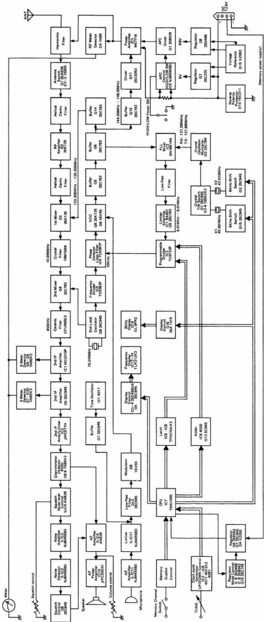
flowchart
graph TD
    A["Squirrel Control Q6 25C945"] --> B["Noise Detector ¼ IC3 NJM4558D"]
    B --> C["Noise Amplifier ¼ IC3 NJM4558D"]
    C --> D["Squelch Noise level Control ¾ IC4 ANB29"]
    D --> E["Discriminator Detector 4550 D8-9 1N60X2"]
    E --> F["2nd IF Amplifier IC2 μPC577H"]
    F --> G["2nd IF Amplifier Q5 2SC945"]
    G --> H["2nd IF Amplifier IC1 MC3310P"]
    H --> I["Ceramic Filter CFU455E2"]
    I --> J["2nd Mixer Q4 2SC763"]
    J --> K["Crystal Filter 10M158B"]
    K --> L["1st Mixer Q3 2SK125"]
    L --> M["Helical Cavity Filter"]
    M --> N["RF Amplifier Q2 2SK125"]
    N --> O["Helical Cavity Filter"]
    O --> P["Antenna Switch Q1 2SA639 D1~3 1SS55"]
    P --> Q["Harmonics Filter"]
    Q --> R["RF Meter Detector D4 1N60"]
    R --> S["Power Amplifier IC1 M57715"]
    S --> T["Driver Q11 2SC2053"]
    T --> U["APC Control HIGH/LOW SW IC5 NJM4558D"]
    U --> V["APC Driver Q1 2S8529"]
    V --> W["Reverse Polarity Protector D10 15CD11"]
    W --> X["Voltage Reference D15 XZ092"]
    X --> Y["DC 13.8V"]
    Z["Squech control"] --> AA["AF Power Amplifier IC10 μPC2002V"]
    AA --> AB["AF Amplifier ¼ IC4 ANB29"]
    AB --> AC["Low Pass Filter Q13 2SC945"]
    AC --> AD["Modulator D8 1SV50"]
    AD --> AE["Display Control Q1-4 2SD46BX4 Q5 2SC945"]
    AE --> AF["Frequency Divider IC5 TC5062P"]
    AF --> AG["Phase Detector Loop Filter IC4 TC5081P"]
    AG --> AH["VCO Q8 2SK125 Q6 1SV50"]
    AH --> AI["Buffer Q9 2SC763"]
    AI --> AJ["Buffer Q6 2SC763"]
    AJ --> AK["Buffer Q14 2SC763"]
    AK --> AL["Buffer Q10 2SC763"]
    AL --> AM["Driver Q11 2SC2053"]
    AM --> AN["Power Amplifier IC1 M57715"]
    AN --> AO["HIGH/LOW Power SW"]
    AO --> AP["RX: 127.295MHz TX: 137.990MHz"]
    AP --> AQ["Limiter Amplifier IC1 BA401 Q5 2SC763"]
    AQ --> AR["Lift IC8·IC9 TP4370AX2"]
    AR --> AS["Adder IC6 4030 Q12 SC945"]
    AS --> AT["Programmable Divider IC3 TC9122P"]
    AT --> AU["Limiter Amplifier IC1 BA401 Q5 2SC763"]
    AU --> AV["Low Pass Filter"]
    AV --> AW["PULL Mixer IC2 SN76514N"]
    AW --> AX["APC Control HIGH/LOW SW IC5 NJM4558D"]
    AX --> AY["RSV"]
    AY --> AZ["Regulator Q7 2SC235"]
    AZ --> BA["Regulator Q8 2SD468"]
    BA --> BB["Reverse Polarity Protector D10 15CD11"]
    BB --> BC["Voltage Reference D15 XZ092"]
    BC --> BD["TUNE"]
    BE["Speaker"] --> BF["AF Power Amplifier IC10 μPC2002V"]
    BF --> BG["Limiter ¾ IC11 NJM4558D"]
    BG --> BH["Low Pass Filter Q13 2SC945"]
    BH --> BI["Modulator D8 1SV50"]
    BI --> BJ["Display Control Q1-4 2SD46BX4 Q5 2SC945"]
    BJ --> BK["Frequency Divider IC12-14 TLR312X3"]
    BK --> BL["5KHz Display D19 GL-9PR2"]
    BL --> BM["Display Control Q16 2SA 1015"]
    BM --> BN["Limiter Amplifier IC1 BA401 Q5 2SC763"]
    BN --> BO["Low Pass Filter"]
    BO --> BP["PULL Mixer IC2 SN76514N"]
    BP --> BQ["RX: 127.295MHz TX: 137.990MHz"]
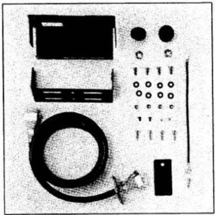
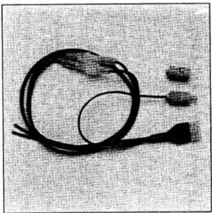
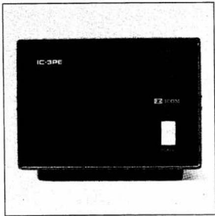
We have prepared a variety of options for the mobile transceiver IC-280E in order to enlarge its use
natural_image
Collection of electronic components including a battery pack, coiled cable, and various connectors (no visible text or symbols)REMOTE CABLE KIT FOR IC-280E
natural_image
Simple line drawing of a coiled tube with three small protrusions (no text or symbols)DC POWER CORD WITH MEMORY BACKUP POWER PLUG
text_image
IC-3PE Z-ROMIC-3PE POWER SUPPLY 13.8V 3A
natural_image
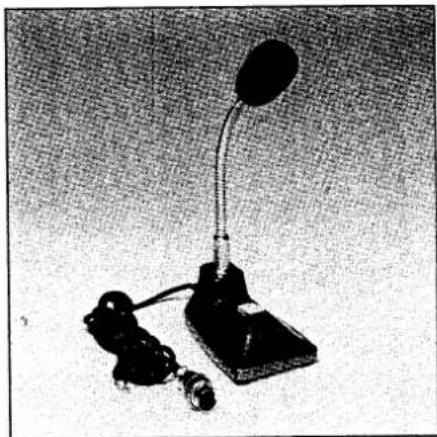
Black-and-white photo of a desk lamp with adjustable arm and base, no visible text or symbolsIC-SM2 DESK MICROPHONE ELECTRET CONDENSER TYPE
natural_image
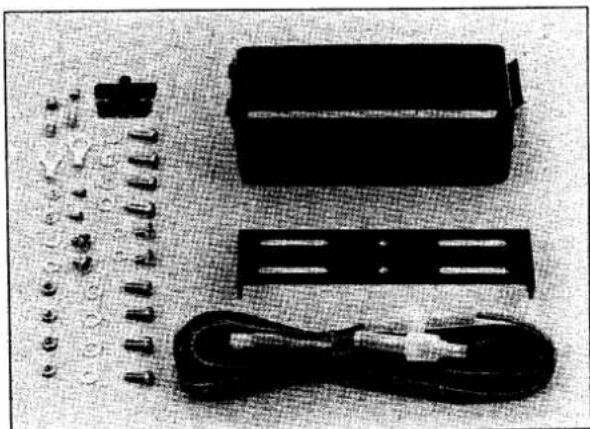
Black electronic device components including a rectangular box, cable, and connector (no visible text or symbols)MOBILE MOUNTING BRACKET (F) FOR IC-280E
MEMO

ICOM
ICOM INCORPORATED
1-6-19, KAMI KURATSUKURI, HIRANO-KU, OSAKA JAPAN